

Best Megasonic Wafer Cleaning System for Enhanced Semiconductor Yield
2026-11-16
Achieving consistent particle removal without damaging delicate device structures remains one of the most underestimated challenges in advanced semiconductor manufacturing. As feature sizes shrink, even trace residues or sub-micron contaminants can quietly erode yield and undermine reliability. Megasonic wafer cleaning has emerged as a compelling solution, using controlled acoustic energy to lift contaminants from wafer surfaces without the mechanical stress of traditional scrubbing. Yet not all megasonic systems deliver the same uniformity, frequency stability, or process control. In this post, we explore the key factors behind an effective megasonic cleaning process and why teams looking to strengthen their yield are paying closer attention to Siansonic as a focused technology partner in this space.
Why Particle Contamination Persists in Advanced Semiconductor Processes
At dimensions where a few atomic layers define the gate stack, particle control has become less about keeping cleanrooms cleaner and more about managing contamination that is indistinguishable from the process itself. Older fabs could rely on air filtration and gowning discipline, but sub-10 nm nodes now face defects from materials that arrive pre-contaminated at levels below conventional inspection thresholds. A ceramic seal that sheds a single 20 nm grain during wafer transfer, or a trace metallic impurity that precipitates during rapid thermal processing, can bridge adjacent lines or alter etch selectivity long before an in-line scanner flags a problem.
The persistence is also built into the equipment. Plasma chambers accumulate polymer deposits that flake after repeated thermal cycling, while electrostatic chucks and lift pins generate wear debris each time a wafer is placed or removed. Some of these particles are generated only after hundreds of RF-hours, making them difficult to reproduce in short-loop tests. Pumps and gas delivery add another layer: precursor lines with dead legs can harbor sub-visible clusters that are released when flow conditions change, so the contamination appears random rather than tied to a single maintenance event.
Metrology compounds the issue. Surface scan tools have improved, but a meaningful defect is now often smaller than the optical scattering cross-section that a reliable monitor can detect at production throughput. Fabs compensate with sampling, which leaves gaps between monitored wafers and monitored chamber conditions. As a result, particle excursions are frequently detected indirectly, through parametric drift or yield loss, after the source has changed or stopped. That lag keeps particle contamination a chronic problem even in facilities with mature contamination control programs.
How Megasonic Acoustic Energy Removes Particles Without Contact
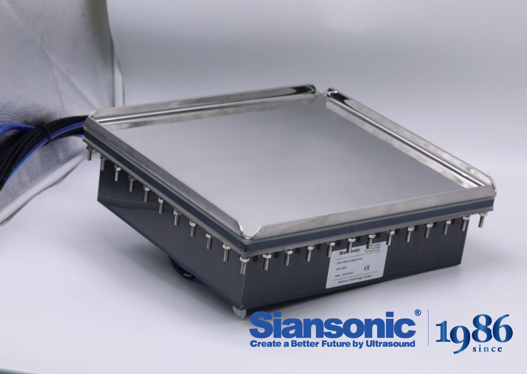
Megasonic cleaning works by turning the fluid itself into a scrubbing force. A transducer bonded to a tank or nozzle launches pressure waves at frequencies around 1 MHz—far above ordinary ultrasonic ranges. In that regime, the oscillating pressure produces a thin, fast-moving acoustic boundary layer at the solid surface. Particles trapped in that layer are hit by sharp velocity gradients and steady acoustic streaming currents. The force is concentrated enough to break van der Waals and electrostatic adhesion, yet the energy is too diffuse to hammer the surface the way an ultrasonic bath would. Because no brush, pad, or spray jet ever makes contact, the wafer stays untouched.
What makes this approach different is its ability to clean inside narrow features without leaving a mechanical signature. On a patterned wafer or a MEMS device, a physical scrubber can snap fins or leave scratches, but a megasonic field wraps into recesses and pushes fluid along the sidewalls. The acoustic pressure also produces a mild lift component that keeps dislodged particles in the moving liquid instead of letting them settle back onto the surface. System tuning matters here: dissolved gas levels, transducer spacing, and power density determine whether the process stays in a gentle streaming mode or tips into cavitation. When the parameters are right, the particle is removed cleanly, with no contact and no residue.
Balancing Cleaning Power and Pattern Damage on Fragile Features
Fragile features rarely tolerate aggressive chemistry, yet lowering mechanical force too far lets residue linger in tight geometries. A useful approach is to map the failure window before committing to a recipe: track line collapse, film loss, or CD shift at increasing power settings, and compare those numbers against particle removal efficiency on the same test structures. That quickly exposes the narrow band where cleaning remains effective without distorting the pattern.
The real balance often sits in parameters that get overlooked in a standard setup. A small change in spray angle, dissolved gas level, or rinse temperature can shift local energy enough to protect a thin fin while still dislodging debris from a high-aspect-ratio trench. Some teams alternate short, higher-energy pulses with longer low-energy rinses, keeping total exposure below the damage threshold while the transient force reaches areas a steady gentle flow would miss.
It also helps to treat the feature as part of a larger stack rather than an isolated line. Underlying films may swell or shrink during drying, and that movement can amplify pattern collapse even when the cleaning step itself looks harmless. A quick check of post-clean defect maps alongside CD-SEM or scatterometry data after a few wafer splits usually reveals whether the recipe is truly balanced or simply hiding damage until later inspection.
Reducing Chemical and Water Use While Maintaining Surface Quality
Cutting back on chemicals and water doesn't have to mean accepting dull floors or streaky metal. In practice, many surface problems come from over-application: too much detergent leaves a film that attracts dirt, and excess rinse water carries residue into grout lines or joints. Starting with dry removal—vacuuming, sweeping, or using a dry microfiber pass—lifts the loose grit before any liquid is introduced. After that, spot treatment can handle most visible marks without treating the entire area. This shifts the routine from "more product" to "product in the right place," which often lowers both chemical inventory and water volume while keeping the surface easier to maintain.
On hard surfaces, the combination of controlled spray rates and high-quality microfiber or soft bristle agitation can preserve, and sometimes improve, the original finish. Lower water flow reduces the chance of slurry being pushed into porous edges, and lower chemical concentration avoids etching or hazing on sensitive coatings. Some teams now track surface condition with a simple gloss meter or a handheld profilometer, checking a few fixed points after cleaning. That kind of measurement makes it easier to reduce inputs gradually instead of making one sudden change and waiting for complaints.
Where water is still needed for rinsing, capture-and-reuse systems can cut total consumption without compromising cleanliness. Filtering rinse water removes suspended solids before the next pass, preventing the buildup of hard-water spots and mineral haze that would otherwise require additional polishing. The result is a quieter shift in operating habits: fewer drums of chemical concentrate, less wastewater to manage, and surfaces that hold their appearance between service intervals rather than fading after each aggressive wash.
Achieving Uniform Cleaning Performance Across the Full Wafer
Uniform cleaning across a wafer rarely fails in obvious ways; it shows up as a scatter of defects near the edge or a stubborn residue patch just off center. The root cause is usually physical rather than chemical. Rotation speed, exhaust flow, and the way rinse water sheets off the surface all create slightly different transport conditions at every radial position. Treating the wafer as a single process zone almost guarantees that the center sees more fresh chemistry while the edge experiences faster drying or thinner liquid coverage.
A more practical approach is to map the clean in radial bands and adjust the arm sweep, flow rate, or dispense timing to flatten those differences. Some lines also vary temperature or dilute the chemistry in zones where the boundary layer is thinner, reducing over-etch at the edge without starving the center. What matters is not the average removal rate but how tightly the result holds from notch to apex.
Verification has to follow the same logic. Full-wafer average particle counts can hide an edge-heavy failure. Mapping defects by radius, or measuring contact angle and trace metal residue on selected die near the edge, center, and mid-radius, gives a much clearer picture. When those values stay within the same narrow window, the clean is genuinely uniform.
Linking Wafer Cleanliness to Higher Final Test Yield
Wafer cleanliness often sits quietly in the background of semiconductor manufacturing, yet its influence on final test yield is far from subtle. A single particle lodged in a critical interconnect can turn into a latent defect that only shows up after packaging, when the cost of failure has multiplied. Teams that treat surface preparation as a routine chore miss the direct line between residue control and the percentage of devices that pass high-temperature operating life tests.
The relationship becomes clearer when you look at probe yield against defect maps from the wafer inspection stage. Cleaner wafers show fewer clusters of edge die failures and tighter distributions in leakage current, both of which translate into stable final test results. Rather than chasing random yield excursions, process engineers can trace many of them back to organic films, dried slurry remnants, or improper rinsing at a single wet bench step.
Practical gains come from tightening cleanroom discipline and rethinking dry times, not from buying another inspection tool. Reducing queue time between cleans, switching to low-residue chemistries, and auditing brush conditioning schedules often move final test yield more than any design tweak. When wafer cleanliness becomes a measured, owned variable instead of an assumption, the downstream improvement shows up not as a spike, but as a sustained rise in the bins that matter.
FAQ
Megasonic systems rely on high-frequency acoustic energy, usually at or above 1 MHz, to create gentle but uniform cavitation across the wafer. That removes particles from deep trenches and narrow patterns without the direct contact of brush scrubbing or the aggressive impact of high-pressure sprays, both of which can damage delicate features.
The transducer sends acoustic waves through the cleaning liquid, producing microstreaming and oscillating bubbles within the thin boundary layer at the wafer surface. Those small-scale forces lift particles away and keep them suspended long enough to be rinsed, which works well in recessed areas where ordinary fluid flow is weak.
Silicon wafers, compound semiconductor substrates, MEMS devices, and advanced logic or memory chips with fragile 3D structures tend to gain the most. Any process where particle residue or pattern collapse is a known yield limiter is a strong candidate for megasonic cleaning.
It can if power density, frequency, chemistry, and exposure time are not properly controlled. Production systems allow those parameters to be tuned so cavitation stays in a controlled, non-destructive range. Patterned wafer testing is usually part of qualification to confirm there is no structural harm.
The liquid does more than transmit sound. Dilute ammonia-peroxide mixtures and other specialized chemistries condition the surface, weaken particle adhesion, and reduce redeposition. The megasonic field then supplies the mechanical energy needed to detach particles without resorting to highly aggressive chemical concentrations.
It lowers defectivity from residues and particles, reduces the chance of pattern damage during cleaning, and delivers more consistent results across wafers and lots. Better surface preparation translates into fewer electrical failures, stronger film adhesion, and more stable final probe yield.
A production-grade tool maintains stable acoustic output across the entire wafer, offers real-time monitoring of power and frequency, and integrates cleanly with automated wafer handling. Lab-scale systems often lack that uniformity and repeatability, which can create unnoticed particle adders or non-uniform cleaning.
Routine checks of transducer output, degas efficiency, filter condition, and tank cleanliness are essential. Cavitation can gradually erode transducer surfaces or shift the acoustic distribution, so periodic calibration and timely replacement of consumables help keep particle removal performance consistent.
Conclusion
As critical dimensions shrink and high-aspect-ratio structures become standard, particle contamination has shifted from a routine nuisance to a direct yield limiter. The adhesion forces holding nanoscale particles on wafer surfaces grow disproportionately relative to particle size, making conventional brush scrubbing or high-pressure jet cleaning less effective and riskier. A megasonic cleaning system addresses this by coupling acoustic energy into a thin liquid film, where controlled cavitation and acoustic streaming generate local shear forces that dislodge particles without physical contact. The real engineering challenge is tuning frequency and power density: excessive energy can collapse fragile gate stacks or photoresist lines, while insufficient energy leaves defects behind. The best systems operate in a narrow process window that removes sub-100 nm particles yet keeps pattern damage below the threshold that impacts device integrity.
Beyond removal efficiency, modern megasonic tools must deliver these results while cutting chemical and water consumption. By using dilute or functionalized chemistries activated by acoustic energy, the cleaning process maintains surface roughness, metal compatibility, and material selectivity without relying on aggressive solvent blends. Uniformity across the full wafer is equally critical; transducer design, frequency sweeping, and bath or nozzle geometry determine whether the edge and center see comparable energy. A system that avoids hot spots and dead zones produces consistent particle removal, which translates directly to lower defect density at electrical test. In advanced fabs, that correlation between post-clean surface quality and final probe yield makes the megasonic cleaner not just a contamination-control step but a measurable contributor to revenue-grade die output.
Contact Us
Contact Person: Ivy Zhang
Email: [email protected]
Tel/WhatsApp: +86 1081502288
Website: https://www.siansonic.com/